 W
WThe metal–oxide–semiconductor field-effect transistor, also known as the metal–oxide–silicon transistor, is a type of insulated-gate field-effect transistor that is fabricated by the controlled oxidation of a semiconductor, typically silicon. The voltage of the covered gate determines the electrical conductivity of the device; this ability to change conductivity with the amount of applied voltage can be used for amplifying or switching electronic signals.
 W
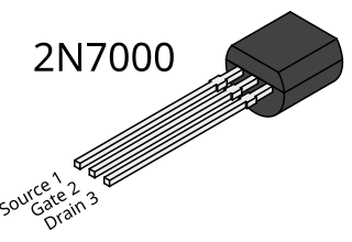
WThe 2N7000 and BS170 are two different N-channel, enhancement-mode MOSFETs used for low-power switching applications, with different lead arrangements and current ratings. They are sometimes listed together on the same datasheet with other variants 2N7002, VQ1000J, and VQ1000P.
 W
WAn active-pixel sensor (APS) is an image sensor where each pixel sensor unit cell has a photodetector and one or more active transistors. In a metal–oxide–semiconductor (MOS) active-pixel sensor, MOS field-effect transistors (MOSFETs) are used as amplifiers. There are different types of APS, including the early NMOS APS and the much more common complementary MOS (CMOS) APS, also known as the CMOS sensor, which is widely used in digital camera technologies such as cell phone cameras, web cameras, most modern digital pocket cameras, most digital single-lens reflex cameras (DSLRs), and mirrorless interchangeable-lens cameras (MILCs). CMOS sensors emerged as an alternative to charge-coupled device (CCD) image sensors and eventually outsold them by the mid-2000s.
 W
WThe metal–oxide–semiconductor field-effect transistor (MOSFET, MOS-FET, or MOS FET), also known as the metal–oxide–silicon transistor (MOS transistor, or MOS), is a type of insulated-gate field-effect transistor (IGFET) that is fabricated by the controlled oxidation of a semiconductor, typically silicon. The voltage of the covered gate determines the electrical conductivity of the device; this ability to change conductivity with the amount of applied voltage can be used for amplifying or switching electronic signals. The MOSFET was invented by Egyptian engineer Mohamed M. Atalla and Korean engineer Dawon Kahng at Bell Labs in 1959. It is the basic building block of modern electronics, and the most frequently manufactured device in history, with an estimated total of 13 sextillion (1.3 × 10²²) MOSFETs manufactured between 1960 and 2018.
 W
WMohamed M. Atalla was an Egyptian-American engineer, physical chemist, cryptographer, inventor and entrepreneur. He was a semiconductor pioneer who made important contributions to modern electronics. He is best known for inventing the MOSFET in 1959, which along with Atalla's earlier surface passivation and thermal oxidation processes, revolutionized the electronics industry. He is also known as the founder of the data security company Atalla Corporation, founded in 1972. He received the Stuart Ballantine Medal and was inducted into the National Inventors Hall of Fame for his important contributions to semiconductor technology as well as data security.
 W
WA field-effect transistor-based biosensor, also known as a biosensor field-effect transistor, field-effect biosensor (FEB), or biosensor MOSFET, is a field-effect transistor that is gated by changes in the surface potential induced by the binding of molecules. When charged molecules, such as biomolecules, bind to the FET gate, which is usually a dielectric material, they can change the charge distribution of the underlying semiconductor material resulting in a change in conductance of the FET channel. A Bio-FET consists of two main compartments: one is the biological recognition element and the other is the field-effect transistor. The BioFET structure is largely based on the ion-sensitive field-effect transistor (ISFET), a type of metal-oxide-semiconductor field-effect transistor (MOSFET) where the metal gate is replaced by an ion-sensitive membrane, electrolyte solution and reference electrode.
 W
WChannel length modulation (CLM) is an effect in field effect transistors, a shortening of the length of the inverted channel region with increase in drain bias for large drain biases. The result of CLM is an increase in current with drain bias and a reduction of output resistance. It is one of several short-channel effects in MOSFET scaling. It also causes distortion in JFET amplifiers.
 W
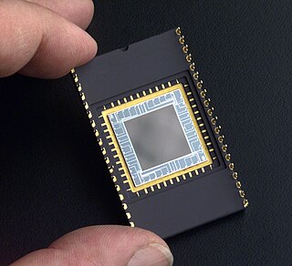
WA charge-coupled device (CCD) is an integrated circuit containing an array of linked, or coupled, capacitors. Under the control of an external circuit, each capacitor can transfer its electric charge to a neighboring capacitor. CCD sensors are a major technology used in digital imaging.
 W
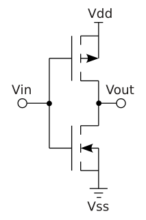
WComplementary metal–oxide–semiconductor (CMOS), also known as complementary-symmetry metal–oxide–semiconductor (COS-MOS), is a type of metal–oxide–semiconductor field-effect transistor (MOSFET) fabrication process that uses complementary and symmetrical pairs of p-type and n-type MOSFETs for logic functions. CMOS technology is used for constructing integrated circuit (IC) chips, including microprocessors, microcontrollers, memory chips, and other digital logic circuits. CMOS technology is also used for analog circuits such as image sensors, data converters, RF circuits, and highly integrated transceivers for many types of communication.
 W
WIn computing, memory is a device or system that is used to store information for immediate use in a computer or related computer hardware and digital electronic devices. The term memory is often synonymous with the term primary storage or main memory. An archaic synonym for memory is store.
 W
WRobert Dennard is an American electrical engineer and inventor.
 W
WIn field-effect transistors (FETS), depletion mode and enhancement mode are two major transistor types, corresponding to whether the transistor is in an ON state or an OFF state at zero gate-source voltage.
 W
WIn integrated circuits, depletion-load NMOS is a form of digital logic family that uses only a single power supply voltage, unlike earlier nMOS logic families that needed more than one different power supply voltage. Although manufacturing these integrated circuits required additional processing steps, improved switching speed and the elimination of the extra power supply made this logic family the preferred choice for many microprocessors and other logic elements.
 W
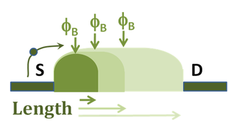
WDrain-induced barrier lowering (DIBL) is a short-channel effect in MOSFETs referring originally to a reduction of threshold voltage of the transistor at higher drain voltages. In a classic planar field-effect transistor with a long channel, the bottleneck in channel formation occurs far enough from the drain contact that it is electrostatically shielded from the drain by the combination of the substrate and gate, and so classically the threshold voltage was independent of drain voltage. In short-channel devices this is no longer true: The drain is close enough to gate the channel, and so a high drain voltage can open the bottleneck and turn on the transistor prematurely.
 W
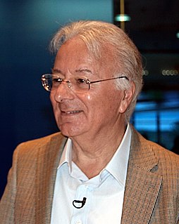
WFederico Faggin is an Italian-American physicist, engineer, inventor and entrepreneur. He is best known for designing the first commercial microprocessor, the Intel 4004. He led the 4004 (MCS-4) project and the design group during the first five years of Intel's microprocessor effort. Faggin also created, while working at Fairchild Semiconductor in 1968, the self-aligned MOS (metal–oxide–semiconductor) silicon-gate technology (SGT), which made possible MOS semiconductor memory chips, CCD image sensors, and the microprocessor. After the 4004, he led development of the Intel 8008 and 8080, using his SGT methodology for random logic chip design, which was essential to the creation of early Intel microprocessors. He was co-founder and CEO of Zilog, the first company solely dedicated to microprocessors, and led the development of the Zilog Z80 and Z8 processors. He was later the co-founder and CEO of Cygnet Technologies, and then Synaptics.
 W
WA FET amplifier is an amplifier that uses one or more field-effect transistors (FETs). The most common type of FET amplifier is the MOSFET amplifier, which uses metal–oxide–semiconductor FETs (MOSFETs). The main advantage of a FET used for amplification is that it has very high input impedance and low output impedance.
 W
WIn physics, the field effect refers to the modulation of the electrical conductivity of a material by the application of an external electric field.
 W
WA fin field-effect transistor (FinFET) is a multigate device, a MOSFET built on a substrate where the gate is placed on two, three, or four sides of the channel or wrapped around the channel, forming a double gate structure. These devices have been given the generic name "finfets" because the source/drain region forms fins on the silicon surface. The FinFET devices have significantly faster switching times and higher current density than planar CMOS technology.
 W
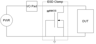
WGrounded-gate NMOS, commonly known as ggNMOS, is an electrostatic discharge (ESD) protection device used within CMOS integrated circuits (ICs). Such devices are used to protect the inputs and outputs of an IC, which can be accessed off-chip and are therefore subject to ESD when touched. An ESD event can deliver a large amount of energy to the chip, potentially destroying input/output circuitry; a ggNMOS device or other ESD protective devices provide a safe path for current to flow, instead of through more sensitive circuitry. ESD protection by means of such devices or other techniques is important to product reliability: 35% of all IC failures in the field are associated with ESD damage.
 W
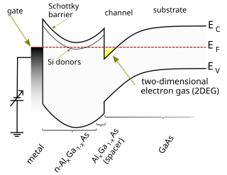
WA high-electron-mobility transistor (HEMT), also known as heterostructure FET (HFET) or modulation-doped FET (MODFET), is a field-effect transistor incorporating a junction between two materials with different band gaps as the channel instead of a doped region. A commonly used material combination is GaAs with AlGaAs, though there is wide variation, dependent on the application of the device. Devices incorporating more indium generally show better high-frequency performance, while in recent years, gallium nitride HEMTs have attracted attention due to their high-power performance. Like other FETs, HEMTs are used in integrated circuits as digital on-off switches. FETs can also be used as amplifiers for large amounts of current using a small voltage as a control signal. Both of these uses are made possible by the FET’s unique current–voltage characteristics. HEMT transistors are able to operate at higher frequencies than ordinary transistors, up to millimeter wave frequencies, and are used in high-frequency products such as cell phones, satellite television receivers, voltage converters, and radar equipment. They are widely used in satellite receivers, in low power amplifiers and in the defense industry.
 W
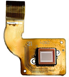
WAn image sensor or imager is a sensor that detects and conveys information used to make an image. It does so by converting the variable attenuation of light waves into signals, small bursts of current that convey the information. The waves can be light or other electromagnetic radiation. Image sensors are used in electronic imaging devices of both analog and digital types, which include digital cameras, camera modules, camera phones, optical mouse devices, medical imaging equipment, night vision equipment such as thermal imaging devices, radar, sonar, and others. As technology changes, electronic and digital imaging tends to replace chemical and analog imaging.
 W
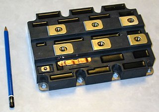
WAn insulated-gate bipolar transistor (IGBT) is a three-terminal power semiconductor device primarily used as an electronic switch, which, as it was developed, came to combine high efficiency and fast switching. It consists of four alternating layers (P–N–P–N) that are controlled by a metal–oxide–semiconductor (MOS) gate structure.
 W
WAn ion-sensitive field-effect transistor (ISFET) is a field-effect transistor used for measuring ion concentrations in solution; when the ion concentration (such as H+, see pH scale) changes, the current through the transistor will change accordingly. Here, the solution is used as the gate electrode. A voltage between substrate and oxide surfaces arises due to an ion sheath. It is a special type of MOSFET (metal-oxide-semiconductor field-effect transistor), and shares the same basic structure, but with the metal gate replaced by an ion-sensitive membrane, electrolyte solution and reference electrode. Invented in 1970, the ISFET was the first biosensor FET (BioFET).
 W
WDawon Kahng was a Korean-American electrical engineer and inventor, known for his work in solid-state electronics. He is best known for inventing the MOSFET, along with his colleague Mohamed Atalla, in 1959. Kahng and Atalla developed both the PMOS and NMOS processes for MOSFET semiconductor device fabrication. The MOSFET is the most widely used type of transistor, and the basic element in most modern electronic equipment.
 W
WThe memory cell is the fundamental building block of computer memory. The memory cell is an electronic circuit that stores one bit of binary information and it must be set to store a logic 1 and reset to store a logic 0. Its value is maintained/stored until it is changed by the set/reset process. The value in the memory cell can be accessed by reading it.
 W
WA metal gate, in the context of a lateral metal-oxide-semiconductor (MOS) stack, is the surface layer separating the transistor unit itself from the attached source— the gate material is made from a metal.
 W
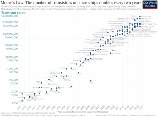
WMoore's law is the observation that the number of transistors in a dense integrated circuit (IC) doubles about every two years. Moore's law is an observation and projection of a historical trend. Rather than a law of physics, it is an empirical relationship linked to gains from experience in production.
 W
WMOSFET Gate Driver is a specialized circuit that is used to drive the gate of power MOSFETs effectively and efficiently in high-speed switching applications. The addition of high MOSFET Gate drivers are the last step if the turn-on is to fully enhance the conducting channel of the MOSFET technology.
 W
WA multigate device, multi-gate MOSFET or multi-gate field-effect transistor (MuGFET) refers to a metal–oxide–semiconductor field-effect transistor (MOSFET) that incorporates more than one gate into a single device. The multiple gates may be controlled by a single gate electrode, wherein the multiple gate surfaces act electrically as a single gate, or by independent gate electrodes. A multigate device employing independent gate electrodes is sometimes called a multiple-independent-gate field-effect transistor (MIGFET). The most widely used multi-gate devices are the FinFET and the GAAFET, which are non-planar transistors, or 3D transistors.
 W
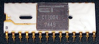
WPMOS or pMOS logic is a family of digital circuits based on p-channel, enhancement mode metal–oxide–semiconductor field-effect transistors (MOSFETs). In the late 1960s and early 1970s, PMOS logic was the dominant semiconductor technology for large-scale integrated circuits before being superseded by NMOS and CMOS devices.
 W
WA power MOSFET is a specific type of metal–oxide–semiconductor field-effect transistor (MOSFET) designed to handle significant power levels. Compared to the other power semiconductor devices, such as an insulated-gate bipolar transistor (IGBT) or a thyristor, its main advantages are high switching speed and good efficiency at low voltages. It shares with the IGBT an isolated gate that makes it easy to drive. They can be subject to low gain, sometimes to a degree that the gate voltage needs to be higher than the voltage under control.
 W
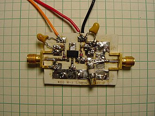
WA radio frequency power amplifier is a type of electronic amplifier that converts a low-power radio-frequency signal into a higher power signal. Typically, RF power amplifiers drive the antenna of a transmitter. Design goals often include gain, power output, bandwidth, power efficiency, linearity, input and output impedance matching, and heat dissipation.
 W
WSemiconductor device fabrication is the process used to manufacture semiconductor devices, typically the metal–oxide–semiconductor (MOS) devices used in the integrated circuit (IC) chips that are present in everyday electrical and electronic devices. It is a multiple-step sequence of photolithographic and chemical processing steps during which electronic circuits are gradually created on a wafer made of pure semiconducting material. Silicon is almost always used, but various compound semiconductors are used for specialized applications.
 W
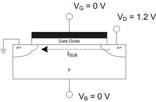
WSubthreshold conduction or subthreshold leakage or subthreshold drain current is the current between the source and drain of a MOSFET when the transistor is in subthreshold region, or weak-inversion region, that is, for gate-to-source voltages below the threshold voltage. The terminology for various degrees of inversion is described by Tsividis.
 W
WIn microfabrication, thermal oxidation is a way to produce a thin layer of oxide on the surface of a wafer. The technique forces an oxidizing agent to diffuse into the wafer at high temperature and react with it. The rate of oxide growth is often predicted by the Deal–Grove model. Thermal oxidation may be applied to different materials, but most commonly involves the oxidation of silicon substrates to produce silicon dioxide.
 W
WA thin-film transistor (TFT) is a special type of metal–oxide–semiconductor field-effect transistor (MOSFET) made by depositing thin films of an active semiconductor layer as well as the dielectric layer and metallic contacts over a supporting substrate. A common substrate is glass, because the primary application of TFTs is in liquid-crystal displays (LCDs). This differs from the conventional bulk MOSFET transistor, where the semiconductor material typically is the substrate, such as a silicon wafer.
 W
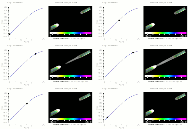
WThe threshold voltage, commonly abbreviated as Vth, of a field-effect transistor (FET) is the minimum gate-to-source voltage VGS (th) that is needed to create a conducting path between the source and drain terminals. It is an important scaling factor to maintain power efficiency.
 W
WAn MOS-controlled thyristor (MCT) is a voltage-controlled fully controllable thyristor, controlled by MOSFETs. It was invented by V.A.K. Temple in 1984, and was principally similar to the earlier insulated-gate bipolar transistor (IGBT). MCTs are similar in operation to GTO thyristors, but have voltage controlled insulated gates. They have two MOSFETs of opposite conductivity types in their equivalent circuits. One is responsible for turn-on and the other for turn-off. A thyristor with only one MOSFET in its equivalent circuit, which can only be turned on, is called an MOS-gated thyristor.
 W
WThe transistor count is the number of transistors in an electronic device. It typically refers to the number of MOSFETs on an integrated circuit (IC) chip, as all modern ICs use MOSFETs. It is the most common measure of IC complexity. The rate at which MOS transistor counts have increased generally follows Moore's law, which observed that the transistor count doubles approximately every two years.
 W
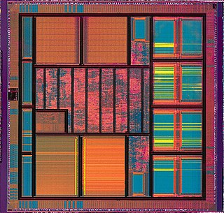
WVery large-scale integration (VLSI) is the process of creating an integrated circuit (IC) by combining millions of MOS transistors onto a single chip. VLSI began in the 1970s when MOS integrated circuit chips were widely adopted, enabling complex semiconductor and telecommunication technologies to be developed. The microprocessor and memory chips are VLSI devices. Before the introduction of VLSI technology, most ICs had a limited set of functions they could perform. An electronic circuit might consist of a CPU, ROM, RAM and other glue logic. VLSI lets IC designers add all of these into one chip.
 W
WA VMOS transistor is a type of MOSFET. VMOS is also used for describing the V-groove shape vertically cut into the substrate material. VMOS is an acronym for "vertical metal oxide semiconductor", or "V-groove MOS".
 W
WA voltage regulator module (VRM), sometimes called processor power module (PPM), is a buck converter that provides a microprocessor the appropriate supply voltage, converting +5 V or +12 V to a much lower voltage required by the CPU, allowing processors with different supply voltage to be mounted on the same motherboard. On personal computer (PC) systems, the VRM is typically made up of power MOSFET devices.