 W
WBroadwell is the fifth model generation of Intel Processor. It's Intel's codename for the 14 nanometer die shrink of its Haswell microarchitecture. It is a "tick" in Intel's tick–tock principle as the next step in semiconductor fabrication. Like some of the previous tick-tock iterations, Broadwell did not completely replace the full range of CPUs from the previous microarchitecture (Haswell), as there were no low-end desktop CPUs based on Broadwell.
 W
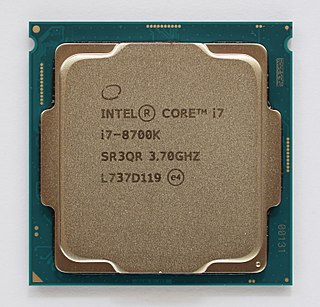
WCoffee Lake is Intel's codename for its eighth generation Core microprocessor family, announced on September 25, 2017. It is manufactured using Intel's second 14 nm process node refinement. Desktop Coffee Lake processors introduced i5 and i7 CPUs featuring six cores and Core i3 CPUs with four cores and no hyperthreading.
 W
WHaswell is the codename for a processor microarchitecture developed by Intel as the "fourth-generation core" successor to the Ivy Bridge. Intel officially announced CPUs based on this microarchitecture on June 4, 2013, at Computex Taipei 2013, while a working Haswell chip was demonstrated at the 2011 Intel Developer Forum. With Haswell, which uses a 22 nm process, Intel also introduced low-power processors designed for convertible or "hybrid" ultrabooks, designated by the "Y" suffix.
 W
WThe Intel Graphics Media Accelerator, or GMA, is a series of integrated graphics processors introduced in 2004 by Intel, replacing the earlier Intel Extreme Graphics series and being succeeded by the Intel HD and Iris Graphics series.
 W
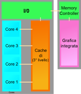
WIntel Graphics Technology (GT) is the collective name for a series of integrated graphics processors (IGPs) produced by Intel that are manufactured on the same package or die as the central processing unit (CPU). It was first introduced in 2010 as Intel HD Graphics.
 W
WIvy Bridge is the codename for the "third generation" of the Intel Core processors. Ivy Bridge is a die shrink to 22 nanometer manufacturing process based on the 32 nanometer Sandy Bridge —see tick–tock model. The name is also applied more broadly to the 22 nm die shrink of the Sandy Bridge microarchitecture based on FinFET ("3D") Tri-Gate transistors, which is also used in the Xeon and Core i7 Ivy Bridge-EX (Ivytown), Ivy Bridge-EP and Ivy Bridge-E microprocessors released in 2013.
 W
WLarrabee is the codename for a cancelled GPGPU chip that Intel was developing separately from its current line of integrated graphics accelerators. It is named after Larrabee State Park in Whatcom County, Washington, near the town of Bellingham. The chip was to be released in 2010 as the core of a consumer 3D graphics card, but these plans were cancelled due to delays and disappointing early performance figures. The project to produce a GPU retail product directly from the Larrabee research project was terminated in May 2010 and its technology was passed on to the Xeon Phi. The Intel MIC multiprocessor architecture announced in 2010 inherited many design elements from the Larrabee project, but does not function as a graphics processing unit; the product is intended as a co-processor for high performance computing.
 W
WNehalem is the codename for an Intel processor microarchitecture released in November 2008. Nehalem was used in the first generation of the Intel Core processors. Nehalem is the successor to the older Core microarchitecture.
The original Pentium microprocessor was introduced by Intel on March 22, 1993. As a direct extension of the 80486 architecture, it was the first superscalar x86 microarchitecture and included dual integer pipelines, a faster floating-point unit, wider data bus, separate code and data caches as well as features for further reduced address calculation latency.
 W
WSandy Bridge is the codename for the microarchitecture used in the "second generation" of the Intel Core processors. The Sandy Bridge microarchitecture is the successor to Nehalem microarchitecture. Intel demonstrated a Sandy Bridge processor in 2009, and released first products based on the architecture in January 2011 under the Core brand.
 W
WSkylake is the codename used by Intel for a processor microarchitecture that was launched in August 2015 succeeding the Broadwell microarchitecture. Skylake is a microarchitecture redesign using the same 14 nm manufacturing process technology as its predecessor, serving as a "tock" in Intel's "tick–tock" manufacturing and design model. According to Intel, the redesign brings greater CPU and GPU performance and reduced power consumption. Skylake CPUs share their microarchitecture with Kaby Lake, Coffee Lake, Cannon Lake, Whiskey Lake, and Comet Lake CPUs.
 W
WWestmere is the code name given to the 32 nm die shrink of Nehalem. While sharing the same CPU sockets, Westmere included Intel HD Graphics, while Nehalem did not.