 W
WIn electronics, a chip carrier is one of several kinds of surface-mount technology packages for integrated circuits. Connections are made on all four edges of a square package; Compared to the internal cavity for mounting the integrated circuit, the package overall size is large.
 W
WA chip scale package or chip-scale package (CSP) is a type of integrated circuit package.
 W
WFan-out wafer-level packaging is an integrated circuit packaging technology, and an enhancement of standard wafer-level packaging (WLP) solutions.
 W
WIntegrated circuits are put into protective packages to allow easy handling and assembly onto printed circuit boards and to protect the devices from damage. A very large number of different types of package exist. Some package types have standardized dimensions and tolerances, and are registered with trade industry associations such as JEDEC and Pro Electron. Other types are proprietary designations that may be made by only one or two manufacturers. Integrated circuit packaging is the last assembly process before testing and shipping devices to customers.
 W
WWafer-level packaging (WLP) is the technology of packaging an integrated circuit while still part of the wafer, in contrast to the more conventional method of slicing the wafer into individual circuits (dice) and then packaging them. WLP is essentially a true chip-scale package (CSP) technology, since the resulting package is practically of the same size as the die. Wafer-level packaging allows integration of wafer fab, packaging, test, and burn-in at wafer level in order to streamline the manufacturing process undergone by a device from silicon start to customer shipment.
 W
WA ball grid array (BGA) is a type of surface-mount packaging used for integrated circuits. BGA packages are used to permanently mount devices such as microprocessors. A BGA can provide more interconnection pins than can be put on a dual in-line or flat package. The whole bottom surface of the device can be used, instead of just the perimeter. The traces connecting the package's leads to the wires or balls which connect the die to package are also on average shorter than with a perimeter-only type, leading to better performance at high speeds.
 W
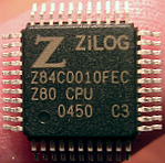
WA quad flat package (QFP) is a surface-mounted integrated circuit package with "gull wing" leads extending from each of the four sides. Socketing such packages is rare and through-hole mounting is not possible. Versions ranging from 32 to 304 pins with a pitch ranging from 0.4 to 1.0 mm are common. Other special variants include low-profile QFP (LQFP) and thin QFP (TQFP).
 W
WIn microelectronics, a dual in-line package, or dual in-line pin package (DIPP) is an electronic component package with a rectangular housing and two parallel rows of electrical connecting pins. The package may be through-hole mounted to a printed circuit board (PCB) or inserted in a socket. The dual-inline format was invented by Don Forbes, Rex Rice and Bryant Rogers at Fairchild R&D in 1964, when the restricted number of leads available on circular transistor-style packages became a limitation in the use of integrated circuits. Increasingly complex circuits required more signal and power supply leads ; eventually microprocessors and similar complex devices required more leads than could be put on a DIP package, leading to development of higher-density chip carriers. Furthermore, square and rectangular packages made it easier to route printed-circuit traces beneath the packages.
WEmbedded Wafer Level Ball Grid Array (eWLB) is a packaging technology for integrated circuits. The package interconnects are applied on an artificial wafer made of silicon chips and a casting compound.
 W
WFlat no-leads packages such as quad-flat no-leads (QFN) and dual-flat no-leads (DFN) physically and electrically connect integrated circuits to printed circuit boards. Flat no-leads, also known as micro leadframe (MLF) and SON, is a surface-mount technology, one of several package technologies that connect ICs to the surfaces of PCBs without through-holes. Flat no-lead is a near chip scale plastic encapsulated package made with a planar copper lead frame substrate. Perimeter lands on the package bottom provide electrical connections to the PCB. Flat no-lead packages include an exposed thermally conductive pad to improve heat transfer out of the IC. Heat transfer can be further facilitated by metal vias in the thermal pad. The QFN package is similar to the quad-flat package (QFP), and a ball grid array (BGA).
 W
WFlatpack is a US military standardized printed-circuit-board surface-mount-component package. The military standard MIL-STD-1835C defines: Flat package (FP). A rectangular or square package with leads parallel to base plane attached on two opposing sides of the package periphery.
 W
WFlip chip, also known as controlled collapse chip connection or its abbreviation, C4, is a method for interconnecting semiconductor devices, such as IC chips and microelectromechanical systems (MEMS), to external circuitry with solder bumps that have been deposited onto the chip pads. The technique was developed by General Electric's Light Military Electronics Dept., Utica, N.Y. The solder bumps are deposited on the chip pads on the top side of the wafer during the final wafer processing step. In order to mount the chip to external circuitry, it is flipped over so that its top side faces down, and aligned so that its pads align with matching pads on the external circuit, and then the solder is reflowed to complete the interconnect. This is in contrast to wire bonding, in which the chip is mounted upright and wires are used to interconnect the chip pads to external circuitry.
 W
WIn electronics manufacturing, integrated circuit packaging is the final stage of semiconductor device fabrication, in which the block of semiconductor material is encapsulated in a supporting case that prevents physical damage and corrosion. The case, known as a "package", supports the electrical contacts which connect the device to a circuit board.
 W
WThe land grid array (LGA) is a type of surface-mount packaging for integrated circuits (ICs) that is notable for having the pins on the socket rather than the integrated circuit. An LGA can be electrically connected to a printed circuit board (PCB) either by the use of a socket or by soldering directly to the board.
 W
WLead frames are the metal structures inside a chip package that carry signals from the die to the outside.
 W
WLow insertion force (LIF) is a technology used in integrated circuit sockets that are designed so the force required to insert or remove a package is low.
 W
WA multi-chip module (MCM) is generically an electronic assembly where multiple integrated circuits, semiconductor dies and/or other discrete components are integrated, usually onto a unifying substrate, so that in use it can be treated as if it were a larger IC. Other terms, such as "hybrid" or "hybrid integrated circuit", also refer to MCMs. The individual ICs that make up an MCM are known as chiplets. Intel and AMD are using MCMs to improve performance and reduce costs, as splitting a large monolithic IC into smaller chiplets allows for easy performance improvements, more ICs per wafer, and improved yield, as smaller dies have a reduced risk of getting destroyed by process variations during semiconductor fabrication. This approach also allows for chiplets to be reused in several products, reduces the amount of time required to design a module compared to designing a monolithic IC, and also reduces the number of bugs that have to be solved during design. However, communication between chiplets consumes more power and has higher latency than components in monolithic ICs. Each chiplet is physically smaller than a conventional monolithic IC die,. An example of MCMs in use for mainstream CPUs is AMD's Zen 2 design.
 W
WThe multi-leaded power package is a style of electronic component package, commonly used for high power integrated circuits, especially for monolithic audio amplifiers. It was derived from single in-line package. The difference is the lead arrangement; multi-leaded power packages usually have the lead bent to zig-zag pattern. Multi-leaded power packages commonly have more than three leads; nine-, thirteen- and fifteen-lead units are common, units with five or seven leads with TO-220 style are also manufactured. A notable characteristic is a metal tab with a hole, used in mounting the case to a heatsink. The physical view of multi-leaded power packages are simply stretched TO-220 packages. Components made in multi-leaded power packages can handle more power than those constructed in TO-220 cases, or even TO3 cases with thermal resistance no less than 1.5 C/W.
 W
WA pin grid array (PGA) is a type of integrated circuit packaging. In a PGA, the package is square or rectangular, and the pins are arranged in a regular array on the underside of the package. The pins are commonly spaced 2.54 mm (0.1") apart, and may or may not cover the entire underside of the package.
WA quad flat package (QFP) is a surface-mounted integrated circuit package with "gull wing" leads extending from each of the four sides. Socketing such packages is rare and through-hole mounting is not possible. Versions ranging from 32 to 304 pins with a pitch ranging from 0.4 to 1.0 mm are common. Other special variants include low-profile QFP (LQFP) and thin QFP (TQFP).
 W
WA small outline integrated circuit (SOIC) is a surface-mounted integrated circuit (IC) package which occupies an area about 30–50% less than an equivalent dual in-line package (DIP), with a typical thickness being 70% less. They are generally available in the same pin-outs as their counterpart DIP ICs. The convention for naming the package is SOIC or SO followed by the number of pins. For example, a 14-pin 4011 would be housed in an SOIC-14 or SO-14 package.
 W
WSurface-mount technology (SMT) is a method in which the electrical components are mounted directly onto the surface of a printed circuit board (PCB). An electrical component mounted in this manner is referred to as a surface-mount device (SMD). In industry, this approach has largely replaced the through-hole technology construction method of fitting components, in large part because SMT allows for increased manufacturing automation which reduces cost and improves quality - It also allows for more components to fit on a given area of substrate. Both technologies can be used on the same board, with the through-hole technology often used for components not suitable for surface mounting such as large transformers and heat-sinked power semiconductors.
WA quad flat package (QFP) is a surface-mounted integrated circuit package with "gull wing" leads extending from each of the four sides. Socketing such packages is rare and through-hole mounting is not possible. Versions ranging from 32 to 304 pins with a pitch ranging from 0.4 to 1.0 mm are common. Other special variants include low-profile QFP (LQFP) and thin QFP (TQFP).
 W
WThin small outline package (TSOP) is a type of surface mount IC package. They are very low-profile and have tight lead spacing.
 W
WThrough-hole technology, refers to the mounting scheme used for electronic components that involves the use of leads on the components that are inserted into holes drilled in printed circuit boards (PCB) and soldered to pads on the opposite side either by manual assembly or by the use of automated insertion mount machines.
 W
WThe universal integrated circuit card (UICC), also known as a SIM card, is the smart card used in mobile terminals in GSM and UMTS networks. The UICC ensures the integrity and security of all kinds of personal data, and it typically holds a few hundred kilobytes.
 W
WThe zig-zag in-line package (ZIP) is a packaging technology for integrated circuits. It was intended as a replacement for dual in-line packaging. A ZIP is an integrated circuit encapsulated in a slab of plastic with 20 or 40 pins, measuring about 3 mm x 30 mm x 10 mm. The package's pins protrude in two rows from one of the long edges. The two rows are staggered by 1.27 mm (0.05"), giving them a zig-zag appearance, and allowing them to be spaced more closely than a rectangular grid would allow. The pins are inserted into holes in a printed circuit board, with the packages standing at right-angles to the board, allowing them to be placed closer together than DIPs of the same size. ZIPs have now been superseded by surface-mount packages such as the thin small-outline packages (TSOPs) but they are still in use.