 W
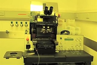
WAn aligner, or mask aligner, is a system that produces integrated circuits (IC) using the photolithography process. It holds the photomask over the silicon wafer while a bright light is shone through the mask and onto the photoresist. The "alignment" refers to the ability to place the mask over precisely the same location repeatedly as the chip goes through multiple rounds of lithography. Aligners were a major part of IC manufacture from the 1960s into the late 1970s, when they began to be replaced by the stepper.
Alvéole is a French company based in Paris and founded in 2010 by Quattrocento, a business accelerator company in the life science field, in collaboration with researchers from the French National Center for Scientific Research with expertise in bioengineering and cell imaging.
 W
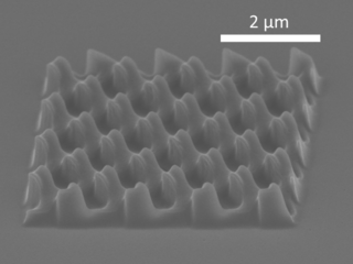
WPhotolithography is a process in removing select portions of thin films used in microfabrication. Microfabrication is the production of parts on the micro- and nano- scale, typically on the surface of silicon wafers, for the production of integrated circuits, microelectromechanical systems (MEMS), solar cells, and other devices. Photolithography makes this process possible through the combined use of hexamethyldisilazane (HMDS), photoresist, spin coating, photomask, an exposure system and other various chemicals. By carefully manipulating these factors it is possible to create nearly any geometry microstructure on the surface of a silicon wafer. The chemical interaction between all the different components and the surface of the silicon wafer makes photolithography an interesting chemistry problem. Current science has been able to create features on the surface of silicon wafers between 1 and 100 μm.
 W
WCymer, LLC., an ASML Holding company, is an American company headquartered in San Diego, California. Cymer is the largest supplier of deep ultraviolet (DUV) light sources used by chipmakers to pattern advanced semiconductor chips or integrated circuits.
 W
WDip pen nanolithography (DPN) is a scanning probe lithography technique where an atomic force microscope (AFM) tip is used to create patterns directly on a range of substances with a variety of inks. A common example of this technique is exemplified by the use of alkane thiolates to imprint onto a gold surface. This technique allows surface patterning on scales of under 100 nanometers. DPN is the nanotechnology analog of the dip pen, where the tip of an atomic force microscope cantilever acts as a "pen," which is coated with a chemical compound or mixture acting as an "ink," and put in contact with a substrate, the "paper."
 W
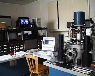
WElectron-beam lithography is the practice of scanning a focused beam of electrons to draw custom shapes on a surface covered with an electron-sensitive film called a resist (exposing). The electron beam changes the solubility of the resist, enabling selective removal of either the exposed or non-exposed regions of the resist by immersing it in a solvent (developing). The purpose, as with photolithography, is to create very small structures in the resist that can subsequently be transferred to the substrate material, often by etching.
 W
WExtreme ultraviolet lithography is a lithography technology using a range of extreme ultraviolet (EUV) wavelengths, roughly spanning a 2% FWHM bandwidth about 13.5 nm.
 W
WImmersion lithography is a photolithography resolution enhancement technique for manufacturing integrated circuits (ICs) that replaces the usual air gap between the final lens and the wafer surface with a liquid medium that has a refractive index greater than one. The resolution is increased by a factor equal to the refractive index of the liquid. Current immersion lithography tools use highly purified water for this liquid, achieving feature sizes below 45 nanometers. ASML and Nikon are currently the only manufacturers of immersion lithography systems.
 W
WLIGA is a German acronym for Lithographie, Galvanoformung, Abformung that describes a fabrication technology used to create high-aspect-ratio microstructures.
 W
WLithography is a method of printing originally based on the immiscibility of oil and water. The printing is from a stone or a metal plate with a smooth surface. It was invented in 1796 by German author and actor Alois Senefelder as a cheap method of publishing theatrical works. Lithography can be used to print text or artwork onto paper or other suitable material.
 W
WLocal oxidation nanolithography (LON) is a tip-based nanofabrication method. It is based on the spatial confinement on an oxidation reaction under the sharp tip of an atomic force microscope.
 W
WMicrocontact printing is a form of soft lithography that uses the relief patterns on a master polydimethylsiloxane (PDMS) stamp to form patterns of self-assembled monolayers (SAMs) of ink on the surface of a substrate through conformal contact as in the case of nanotransfer printing (nTP). Its applications are wide-ranging including microelectronics, surface chemistry and cell biology.
 W
WMicropatterning is the art of miniaturisation of patterns. Especially used for electronics, it has recently become a standard in biomaterials engineering and for fundamental research on cellular biology by mean of soft lithography. It generally uses photolithography methods but many techniques have been developed.
 W
WMultiphoton lithography of polymer templates has been known for years by the photonic crystal community. Similar to standard photolithography techniques, structuring is accomplished by illuminating negative-tone or positive-tone photoresists via light of a well-defined wavelength. The fundamental difference is, however, the avoidance of reticles. Instead, two-photon absorption is utilized to induce a dramatic change in the solubility of the resist for appropriate developers.
 W
WMultiple patterning is a class of technologies for manufacturing integrated circuits (ICs), developed for photolithography to enhance the feature density. It is expected to be necessary for the 10 nm and 7 nm node semiconductor processes and beyond. The premise is that a single lithographic exposure may not be enough to provide sufficient resolution. Hence additional exposures would be needed, or else positioning patterns using etched feature sidewalls would be necessary.
 W
WA nanofountain probe (NFP) is a device for 'drawing' micropatterns of liquid chemicals at extremely small resolution. An NFP contains a cantilevered micro-fluidic device terminated in a nanofountain. The embedded microfluidics facilitates rapid and continuous delivery of molecules from the on-chip reservoirs to the fountain tip. When the tip is brought into contact with the substrate, a liquid meniscus forms, providing a path for molecular transport to the substrate. By controlling the geometry of the meniscus through hold time and deposition speed, various inks and biomolecules could be patterned on a surface, with sub 100 nm resolution.
 W
WNanoimprint lithography (NIL) is a method of fabricating nanometer scale patterns. It is a simple nanolithography process with low cost, high throughput and high resolution. It creates patterns by mechanical deformation of imprint resist and subsequent processes. The imprint resist is typically a monomer or polymer formulation that is cured by heat or UV light during the imprinting. Adhesion between the resist and the template is controlled to allow proper release.
 W
WOptical proximity correction (OPC) is a photolithography enhancement technique commonly used to compensate for image errors due to diffraction or process effects. The need for OPC is seen mainly in the making of semiconductor devices and is due to the limitations of light to maintain the edge placement integrity of the original design, after processing, into the etched image on the silicon wafer. These projected images appear with irregularities such as line widths that are narrower or wider than designed, these are amenable to compensation by changing the pattern on the photomask used for imaging. Other distortions such as rounded corners are driven by the resolution of the optical imaging tool and are harder to compensate for. Such distortions, if not corrected for, may significantly alter the electrical properties of what was being fabricated. Optical proximity correction corrects these errors by moving edges or adding extra polygons to the pattern written on the photomask. This may be driven by pre-computed look-up tables based on width and spacing between features or by using compact models to dynamically simulate the final pattern and thereby drive the movement of edges, typically broken into sections, to find the best solution,. The objective is to reproduce on the semiconductor wafer, as well as possible, the original layout drawn by the designer.
 W
WPDMS stamps are pieces of polydimethylsiloxane (PDMS), a silicone, that have been patterned usually against a master to form a relief pattern used in soft lithography. This PDMS stamp can be used in either its current form as a relief surface for techniques such as microcontact printing or can also be attached to an external source by tubing so that liquid may be passed through channels on its surface. In this second case it will often be laminated to a surface so that chemistry can be performed on that surface producing a pattern of the PDMS stamp on to the surface. Alternatively a PDMS stamp can be laminated to a second piece of PDMS to form a contained device. It is possible to pattern PDMS with nanometre resolution. PDMS stamps can be procured from some commercial sources such as Research Micro Stamps. Many techniques have been developed to modify the basic setups to perform a range of tasks such as assays on small volumes. These kinds of devices are often referred to as microfluidic devices. Because of the small dimensions of these devices flow is laminar not turbulent which can lead to many useful properties; however, this reduces the ability of fluid streams to mix.
 W
WPhase-shift masks are photomasks that take advantage of the interference generated by phase differences to improve image resolution in photolithography. There exist alternating and attenuated phase shift masks. A phase-shift mask relies on the fact that light passing through a transparent media will undergo a phase change as a function of its optical thickness.
 W
WA photomask is an opaque plate with holes or transparencies that allow light to shine through in a defined pattern. They are commonly used in photolithography and the production of integrated circuits in particular. Masks are used to produce a pattern on a substrate, normally a thin slice of silicon known as a wafer in the case of chip manufacturing. Several masks are used in turn, each one reproducing a layer of the completed design, and together they are known as a mask set.
 W
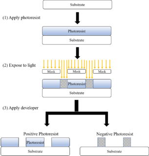
WA photoresist is a light-sensitive material used in several processes, such as photolithography and photoengraving, to form a patterned coating on a surface. This process is crucial in the electronic industry.
 W
WIn technology, soft lithography is a family of techniques for fabricating or replicating structures using "elastomeric stamps, molds, and conformable photomasks". It is called "soft" because it uses elastomeric materials, most notably PDMS.
 W
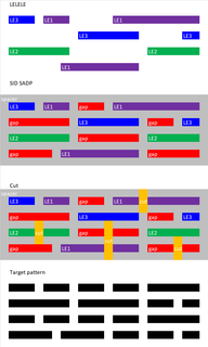
WSpacer patterning is a technique employed for patterning features with linewidths smaller than can be achieved by conventional lithography. In the most general sense, the spacer is a layer that is deposited over a pre-patterned feature, often called the mandrel. The spacer is subsequently etched back so that the spacer portion covering the mandrel is etched away while the spacer portion on the sidewall remains. The mandrel may then be removed, leaving two spacers for each mandrel. The spacers may be further trimmed to narrower widths, especially to act as mandrels for a subsequent 2nd spacer formation. Hence this is a readily practiced form of multiple patterning. Alternatively, one of the two spacers may be removed and the remaining one trimmed to a much smaller final linewidth. Whereas immersion lithography has a resolution of ~40 nm lines and spaces, spacer patterning may be applied to attain 20 nm. This resolution improvement technique is also known as Self-Aligned Double Patterning (SADP). SADP may be re-applied for even higher resolution, and has already been demonstrated for 15 nm NAND flash memory. Spacer patterning has also been adopted for sub-20 nm logic nodes, e.g., 14 nm and 10 nm.
 W
WA stepper is a device used in the manufacture of integrated circuits (ICs) that is similar in operation to a slide projector or a photographic enlarger. The term "stepper" is short for step-and-repeat camera. Steppers are an essential part of the complex process, called photolithography, that creates millions of microscopic circuit elements on the surface of chips of silicon. These chips form the heart of ICs such as computer processors, memory chips, and many other devices.
 W
WThermal scanning probe lithography (t-SPL) is a form of scanning probe lithography (SPL) whereby material is structured on the nanoscale using scanning probes, primarily through the application of thermal energy.
 W
WX-ray lithography, is a process used in electronic industry to selectively remove parts of a thin film. It uses X-rays to transfer a geometric pattern from a mask to a light-sensitive chemical photoresist, or simply "resist," on the substrate. A series of chemical treatments then engraves the produced pattern into the material underneath the photoresist.