 W
WAnderson's rule is used for the construction of energy band diagrams of the heterojunction between two semiconductor materials. Anderson's rule states that when constructing an energy band diagram, the vacuum levels of the two semiconductors on either side of the heterojunction should be aligned.
 W
WIn solid-state physics of semiconductors, a band diagram is a diagram plotting various key electron energy levels as a function of some spatial dimension, which is often denoted x. These diagrams help to explain the operation of many kinds of semiconductor devices and to visualize how bands change with position. The bands may be coloured to distinguish level filling.
 W
WIn physics, the field effect refers to the modulation of the electrical conductivity of a material by the application of an external electric field.
 W
WA homojunction is a semiconductor interface that occurs between layers of similar semiconductor material, these materials have equal band gaps but typically have different doping. In most practical cases a homojunction occurs at the interface between an n-type and p-type semiconductor such as silicon, this is called a p-n junction.
 W
WA metal gate, in the context of a lateral metal-oxide-semiconductor (MOS) stack, is just that—the gate material is made from a metal.
 W
WA p–n junction is a boundary or interface between two types of semiconductor materials, p-type and n-type, inside a single crystal of semiconductor. The "p" (positive) side contains an excess of holes, while the "n" (negative) side contains an excess of electrons in the outer shells of the electrically neutral atoms there. This allows electrical current to pass through the junction only in one direction. The p-n junction is created by doping, for example by ion implantation, diffusion of dopants, or by epitaxy. If two separate pieces of material were used, this would introduce a grain boundary between the semiconductors that would severely inhibit its utility by scattering the electrons and holes.
 W
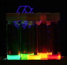
WQuantum dots (QDs) are semiconductor particles a few nanometres in size, having optical and electronic properties that differ from larger particles due to quantum mechanics. They are a central topic in nanotechnology. When the quantum dots are illuminated by UV light, an electron in the quantum dot can be excited to a state of higher energy. In the case of a semiconducting quantum dot, this process corresponds to the transition of an electron from the valence band to the conductance band. The excited electron can drop back into the valence band releasing its energy by the emission of light. This light emission (photoluminescence) is illustrated in the figure on the right. The color of that light depends on the energy difference between the conductance band and the valence band.
 W
WQuantum heterostructure is a heterostructure in a substrate, where size restricts the movements of the charge carriers forcing them into a quantum confinement. This leads to the formation of a set of discrete energy levels at which the carriers can exist. Quantum heterostructures have sharper density of states than structures of more conventional sizes.
 W
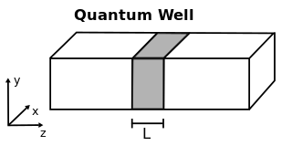
WA quantum well is a potential well with only discrete energy values.
 W
WA Schottky barrier, named after Walter H. Schottky, is a potential energy barrier for electrons formed at a metal–semiconductor junction. Schottky barriers have rectifying characteristics, suitable for use as a diode. One of the primary characteristics of a Schottky barrier is the Schottky barrier height, denoted by ΦB. The value of ΦB depends on the combination of metal and semiconductor.
 W
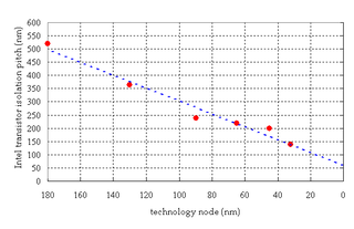
WShallow trench isolation (STI), also known as box isolation technique, is an integrated circuit feature which prevents electric current leakage between adjacent semiconductor device components. STI is generally used on CMOS process technology nodes of 250 nanometers and smaller. Older CMOS technologies and non-MOS technologies commonly use isolation based on LOCOS.