 W
WCompliant bonding is used to connect gold wires to electrical components such as integrated circuit "chips". It was invented by Alexander Coucoulas in the 1960s. The bond is formed well below the melting point of the mating gold surfaces and is therefore referred to as a solid-state type bond. The compliant bond is formed by transmitting heat and pressure to the bond region through a relatively thick indentable or compliant medium, generally an aluminum tape.
 W
WEtching is used in microfabrication to chemically remove layers from the surface of a wafer during manufacturing. Etching is a critically important process module, and every wafer undergoes many etching steps before it is complete.
 W
WEutectic bonding, also referred to as eutectic soldering, describes a wafer bonding technique with an intermediate metal layer that can produce a eutectic system. Those eutectic metals are alloys that transform directly from solid to liquid state, or vice versa from liquid to solid state, at a specific composition and temperature without passing a two-phase equilibrium, i.e. liquid and solid state. The fact that the eutectic temperature can be much lower than the melting temperature of the two or more pure elements can be important in eutectic bonding.
 W
WFan-out wafer-level packaging is an integrated circuit packaging technology, and an enhancement of standard wafer-level packaging (WLP) solutions.
 W
WIn physics, the field effect refers to the modulation of the electrical conductivity of a material by the application of an external electric field.
 W
WIon implantation is a low-temperature process by which ions of one element are accelerated into a solid target, thereby changing the physical, chemical, or electrical properties of the target. Ion implantation is used in semiconductor device fabrication and in metal finishing, as well as in materials science research. The ions can alter the elemental composition of the target if they stop and remain in the target. Ion implantation also causes chemical and physical changes when the ions impinge on the target at high energy. The crystal structure of the target can be damaged or even destroyed by the energetic collision cascades, and ions of sufficiently high energy can cause nuclear transmutation.
 W
WSmart cut is a technological process that enables the transfer of very fine layers of crystalline silicon material onto a mechanical support. It was invented by Michel Bruel of CEA-Leti, and is protected by US patent 5374564. The application of this technological procedure is mainly in the production of silicon-on-insulator (SOI) wafer substrates.
 W
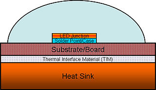
WHigh power light-emitting diodes (LEDs) can use 350 milliwatts or more in a single LED. Most of the electricity in an LED becomes heat rather than light. If this heat is not removed, the LEDs run at high temperatures, which not only lowers their efficiency, but also makes the LED less reliable. Thus, thermal management of high power LEDs is a crucial area of research and development. It is necessary to limit both the junction and the phosphor particles temperatures to a value that will guarantee the desired LED lifetime.
 W
WIn microfabrication, thermal oxidation is a way to produce a thin layer of oxide on the surface of a wafer. The technique forces an oxidizing agent to diffuse into the wafer at high temperature and react with it. The rate of oxide growth is often predicted by the Deal–Grove model. Thermal oxidation may be applied to different materials, but most commonly involves the oxidation of silicon substrates to produce silicon dioxide.
 W
WTransient photocurrent (TPC) is a measurement technique, typically employed in the physics of thin film semiconductors. TPC allows to study the time-dependent extraction of charges generated by photovoltaic effect in semiconductor devices, such as solar cells.
 W
WWafer-level packaging (WLP) is the technology of packaging an integrated circuit while still part of the wafer, in contrast to the more conventional method of slicing the wafer into individual circuits (dice) and then packaging them. WLP is essentially a true chip-scale package (CSP) technology, since the resulting package is practically of the same size as the die. Wafer-level packaging allows integration of wafer fab, packaging, test, and burn-in at wafer level in order to streamline the manufacturing process undergone by a device from silicon start to customer shipment.
 W
WWire drawing is a metalworking process used to reduce the cross-section of a wire by pulling the wire through a single, or series of, drawing die(s). There are many applications for wire drawing, including electrical wiring, cables, tension-loaded structural components, springs, paper clips, spokes for wheels, and stringed musical instruments. Although similar in process, drawing is different from extrusion, because in drawing the wire is pulled, rather than pushed, through the die. Drawing is usually performed at room temperature, thus classified as a cold working process, but it may be performed at elevated temperatures for large wires to reduce forces.