 W
WBio-MEMS is an abbreviation for biomedical microelectromechanical systems. Bio-MEMS have considerable overlap, and is sometimes considered synonymous, with lab-on-a-chip (LOC) and micro total analysis systems (μTAS). Bio-MEMS is typically more focused on mechanical parts and microfabrication technologies made suitable for biological applications. On the other hand, lab-on-a-chip is concerned with miniaturization and integration of laboratory processes and experiments into single chips. In this definition, lab-on-a-chip devices do not strictly have biological applications, although most do or are amenable to be adapted for biological purposes. Similarly, micro total analysis systems may not have biological applications in mind, and are usually dedicated to chemical analysis. A broad definition for bio-MEMS can be used to refer to the science and technology of operating at the microscale for biological and biomedical applications, which may or may not include any electronic or mechanical functions. The interdisciplinary nature of bio-MEMS combines material sciences, clinical sciences, medicine, surgery, electrical engineering, mechanical engineering, optical engineering, chemical engineering, and biomedical engineering. Some of its major applications include genomics, proteomics, molecular diagnostics, point-of-care diagnostics, tissue engineering, single cell analysis and implantable microdevices.
 W
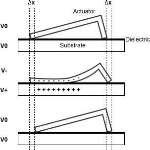
WComb-drives are microelectromechanical actuators, often used as linear actuators, which utilize electrostatic forces that act between two electrically conductive combs. Comb drive actuators typically operate at the micro- or nanometer scale and are generally manufactured by bulk micromachining or surface micromachining a silicon wafer substrate.
 W
WDeformable mirrors (DM) are mirrors whose surface can be deformed, in order to achieve wavefront control and correction of optical aberrations. Deformable mirrors are used in combination with wavefront sensors and real-time control systems in adaptive optics. In 2006 they found a new use in femtosecond pulse shaping.
 W
WThe digital micromirror device, or DMD, is the microoptoelectromechanical system (MOEMS) that is the core of the trademarked DLP projection technology from Texas Instruments (TI). Texas Instrument's DMD was created by solid state physicist and TI Fellow Emeritus Dr. Larry Hornbeck in 1987. However, the technology goes back to 1973 with Harvey C. Nathanson's use of millions of microscopically small moving mirrors to create a video display of the type now found in digital projectors.
 W
WDip pen nanolithography (DPN) is a scanning probe lithography technique where an atomic force microscope (AFM) tip is used to create patterns directly on a range of substances with a variety of inks. A common example of this technique is exemplified by the use of alkane thiolates to imprint onto a gold surface. This technique allows surface patterning on scales of under 100 nanometers. DPN is the nanotechnology analog of the dip pen, where the tip of an atomic force microscope cantilever acts as a "pen," which is coated with a chemical compound or mixture acting as an "ink," and put in contact with a substrate, the "paper."
 W
WA DNA microarray is a collection of microscopic DNA spots attached to a solid surface. Scientists use DNA microarrays to measure the expression levels of large numbers of genes simultaneously or to genotype multiple regions of a genome. Each DNA spot contains picomoles of a specific DNA sequence, known as probes. These can be a short section of a gene or other DNA element that are used to hybridize a cDNA or cRNA sample under high-stringency conditions. Probe-target hybridization is usually detected and quantified by detection of fluorophore-, silver-, or chemiluminescence-labeled targets to determine relative abundance of nucleic acid sequences in the target. The original nucleic acid arrays were macro arrays approximately 9 cm × 12 cm and the first computerized image based analysis was published in 1981. It was invented by Patrick O. Brown. An example of its application is in SNPs arrays for polymorphisms in cardiovascular diseases, cancer, pathogens and GWAS analysis. Also for identification of structural variations and measurement of gene expression.
 W
WEtching is used in microfabrication to chemically remove layers from the surface of a wafer during manufacturing. Etching is a critically important process module, and every wafer undergoes many etching steps before it is complete.
 W
WThe GP5 is a co-processor accelerator built to accelerate discrete belief propagation on factor graphs and other large-scale tensor product operations for machine learning. It is related to, and anticipated by a number of years, the Google Tensor Processing Unit
 W
WIndustrial computed tomography (CT) scanning is any computer-aided tomographic process, usually X-ray computed tomography, that uses irradiation to produce three-dimensional internal and external representations of a scanned object. Industrial CT scanning has been used in many areas of industry for internal inspection of components. Some of the key uses for industrial CT scanning have been flaw detection, failure analysis, metrology, assembly analysis and reverse engineering applications. Just as in medical imaging, industrial imaging includes both nontomographic radiography and computed tomographic radiography.
 W
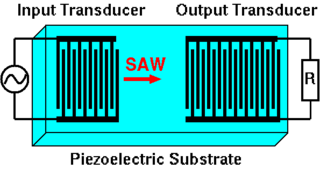
WAn interdigital transducer (IDT) is a device that consists of two interlocking comb-shaped arrays of metallic electrodes. These metallic electrodes are deposited on the surface of a piezoelectric substrate, such as quartz or lithium niobate, to form a periodic structure.
 W
WIon tracks are damage-trails created by swift heavy ions penetrating through solids, which may be sufficiently-contiguous for chemical etching in a variety of crystalline, glassy, and/or polymeric solids. They are associated with cylindrical damage-regions several nanometers in diameter and can be studied by Rutherford backscattering spectrometry (RBS), transmission electron microscopy (TEM), small-angle neutron scattering (SANS), small-angle X-ray scattering (SAXS) or gas permeation.
 W
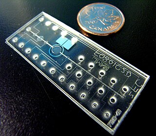
WLab on a Chip is a peer-reviewed scientific journal which publishes original (primary) research and review articles on any aspect of miniaturisation at the micro and nano scale. Lab on a Chip is published twice monthly by the Royal Society of Chemistry (RSC) and the editor-in-chief is Abraham Lee. The journal was established in 2001 and hosts other RSC publications: Highlights in Chemical Technology and Highlights in Chemical Biology. According to the Journal Citation Reports, the journal has a 2016 impact factor of 6.
 W
WLIGA is a German acronym for Lithographie, Galvanoformung, Abformung that describes a fabrication technology used to create high-aspect-ratio microstructures.
 W
WMicrobotics is the field of miniature robotics, in particular mobile robots with characteristic dimensions less than 1 mm. The term can also be used for robots capable of handling micrometer size components.
 W
WMicroelectromechanical systems (MEMS), also written as micro-electro-mechanical systems and the related micromechatronics and microsystems constitute the technology of microscopic devices, particularly those with moving parts. They merge at the nanoscale into nanoelectromechanical systems (NEMS) and nanotechnology. MEMS are also referred to as micromachines in Japan and microsystem technology (MST) in Europe.
 W
WMicrofabrication is the process of fabricating miniature structures of micrometre scales and smaller. Historically, the earliest microfabrication processes were used for integrated circuit fabrication, also known as "semiconductor manufacturing" or "semiconductor device fabrication". In the last two decades microelectromechanical systems (MEMS), microsystems, micromachines and their subfields, microfluidics/lab-on-a-chip, optical MEMS, RF MEMS, PowerMEMS, BioMEMS and their extension into nanoscale have re-used, adapted or extended microfabrication methods. Flat-panel displays and solar cells are also using similar techniques.
 W
WA microlens is a small lens, generally with a diameter less than a millimetre (mm) and often as small as 10 micrometres (µm). The small sizes of the lenses means that a simple design can give good optical quality but sometimes unwanted effects arise due to optical diffraction at the small features. A typical microlens may be a single element with one plane surface and one spherical convex surface to refract the light. Because micro-lenses are so small, the substrate that supports them is usually thicker than the lens and this has to be taken into account in the design. More sophisticated lenses may use aspherical surfaces and others may use several layers of optical material to achieve their design performance.
 W
WMicromachines are mechanical objects that are fabricated in the same general manner as integrated circuits. They are generally considered to be between 100 nanometres to 100 micrometres in size, though that is debatable. The applications of micromachines include accelerometers that detect when a car has hit an object and trigger an airbag. Complex systems of gears and levers are another application.
 W
WMicropatterning is the art of miniaturisation of patterns. Especially used for electronics, it has recently become a standard in biomaterials engineering and for fundamental research on cellular biology by mean of soft lithography. It generally uses photolithography methods but many techniques have been developed.
 W
WMicropumps are devices that can control and manipulate small fluid volumes. Although any kind of small pump is often referred to as micropump, a more accurate definition restricts this term to pumps with functional dimensions in the micrometer range. Such pumps are of special interest in microfluidic research, and have become available for industrial product integration in recent years. Their miniaturized overall size, potential cost and improved dosing accuracy compared to existing miniature pumps fuel the growing interest for this innovative kind of pump.
 W
WA microreactor or microstructured reactor or microchannel reactor is a device in which chemical reactions take place in a confinement with typical lateral dimensions below 1 mm; the most typical form of such confinement are microchannels. Microreactors are studied in the field of micro process engineering, together with other devices in which physical processes occur. The microreactor is usually a continuous flow reactor. Microreactors offer many advantages over conventional scale reactors, including vast improvements in energy efficiency, reaction speed and yield, safety, reliability, scalability, on-site/on-demand production, and a much finer degree of process control.
 W
WA microscanner, or micro scanning mirror, is a microoptoelectromechanical system (MOEMS) in the category of micromirror actuators for dynamic light modulation. Depending upon the type of microscanner the modulatory movement of a single mirror can be either translatory or rotational, on one or two axes. In the first case, a phase shifting effect takes place. In the second case, the incident light wave is deflected.
 W
WMinatec is a vast complex specializing in micro-nano technologies in Grenoble, France.
 W
WA nanofountain probe (NFP) is a device for 'drawing' micropatterns of liquid chemicals at extremely small resolution. An NFP contains a cantilevered micro-fluidic device terminated in a nanofountain. The embedded microfluidics facilitates rapid and continuous delivery of molecules from the on-chip reservoirs to the fountain tip. When the tip is brought into contact with the substrate, a liquid meniscus forms, providing a path for molecular transport to the substrate. By controlling the geometry of the meniscus through hold time and deposition speed, various inks and biomolecules could be patterned on a surface, with sub 100 nm resolution.
 W
WA scratch drive actuator (SDA) is a microelectromechanical system device that converts electrical energy into one-dimensional motion.
 W
WThe Semi-Conductor Laboratory, Mohali (SCL) is a research institute of the Department of Space, Government of India. Its aims include research and development in the field of semiconductor technology.
 W
WSmart cut is a technological process that enables the transfer of very fine layers of crystalline silicon material onto a mechanical support. It was invented by Michel Bruel of CEA-Leti, and is protected by US patent 5374564. The application of this technological procedure is mainly in the production of silicon-on-insulator (SOI) wafer substrates.
 W
WSupercritical drying, also known as critical point drying, is a process to remove liquid in a precise and controlled way. It is useful in the production of microelectromechanical systems (MEMS), the drying of spices, the production of aerogel, the decaffeination of coffee and in the preparation of biological specimens for scanning electron microscopy.
 W
WA surface acoustic wave (SAW) is an acoustic wave traveling along the surface of a material exhibiting elasticity, with an amplitude that typically decays exponentially with depth into the material.
 W
WA system in a package (SiP) or system-in-package is a number of integrated circuits enclosed in one or more chip carrier packages that may be stacked using package on package. The SiP performs all or most of the functions of an electronic system, and is typically used inside a mobile phone, digital music player, etc. Dies containing integrated circuits may be stacked vertically on a substrate. They are internally connected by fine wires that are bonded to the package. Alternatively, with a flip chip technology, solder bumps are used to join stacked chips together. A SiP is like a system on a chip (SoC) but less tightly integrated and not on a single semiconductor die.
 W
WA system on a chip is an integrated circuit that integrates all or most components of a computer or other electronic system. These components almost always include a central processing unit (CPU), memory, input/output ports and secondary storage, often alongside other components such as radio modems and a GPU – all on a single substrate or microchip. It may contain digital, analog, mixed-signal, and often radio frequency signal processing functions.
 W
WIn microfabrication, thermal oxidation is a way to produce a thin layer of oxide on the surface of a wafer. The technique forces an oxidizing agent to diffuse into the wafer at high temperature and react with it. The rate of oxide growth is often predicted by the Deal–Grove model. Thermal oxidation may be applied to different materials, but most commonly involves the oxidation of silicon substrates to produce silicon dioxide.
 W
WA trojan wave packet is a wave packet that is nonstationary and nonspreading. It is part of an artificially created system that consists of a nucleus and one or more electron wave packets, and that is highly excited under a continuous electromagnetic field.
 W
WX-ray microtomography, like tomography and X-ray computed tomography, uses X-rays to create cross-sections of a physical object that can be used to recreate a virtual model without destroying the original object. The prefix micro- is used to indicate that the pixel sizes of the cross-sections are in the micrometre range. These pixel sizes have also resulted in the terms high-resolution X-ray tomography, micro–computed tomography, and similar terms. Sometimes the terms high-resolution CT (HRCT) and micro-CT are differentiated, but in other cases the term high-resolution micro-CT is used. Virtually all tomography today is computed tomography.