 W
WA semiconductor material has an electrical conductivity value falling between that of a conductor, such as metallic copper, and an insulator, such as glass. Its resistivity falls as its temperature rises; metals behave in the opposite way. Its conducting properties may be altered in useful ways by introducing impurities ("doping") into the crystal structure. When two differently doped regions exist in the same crystal, a semiconductor junction is created. The behavior of charge carriers, which include electrons, ions and electron holes, at these junctions is the basis of diodes, transistors and most modern electronics. Some examples of semiconductors are silicon, germanium, gallium arsenide, and elements near the so-called "metalloid staircase" on the periodic table. After silicon, gallium arsenide is the second-most common semiconductor and is used in laser diodes, solar cells, microwave-frequency integrated circuits, and others. Silicon is a critical element for fabricating most electronic circuits.
 W
WThe field-effect transistor (FET) is a type of transistor that uses an electric field to control the flow of current in a semiconductor. FETs are devices with three terminals: source, gate, and drain. FETs control the flow of current by the application of a voltage to the gate, which in turn alters the conductivity between the drain and source.
 W
WWeili Dai is a Chinese-born American businesswoman. She is the co-founder, former director, and former president of Marvell Technology Group. Dai is a successful women entrepreneur, and is the only female co-founder of a major semiconductor company. As of 2015, she is listed as the 95th richest woman in the world by Forbes. Her estimated networth was US$930 million in mid-2018.
 W
WIn physics, the field effect refers to the modulation of the electrical conductivity of a material by the application of an external electric field.
 W
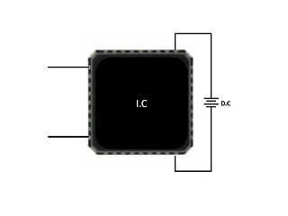
WHigh-temperature operating life (HTOL) is a reliability test applied to integrated circuits (ICs) to determine their intrinsic reliability. This test stresses the IC at an elevated temperature, high voltage and dynamic operation for a predefined period of time. The IC is usually monitored under stress and tested at intermediate intervals. This reliability stress test is sometimes referred to as a "lifetime test", "device life test" or "extended burn in test" and is used to trigger potential failure modes and assess IC lifetime.
 W
WImpact ionization is the process in a material by which one energetic charge carrier can lose energy by the creation of other charge carriers. For example, in semiconductors, an electron with enough kinetic energy can knock a bound electron out of its bound state and promote it to a state in the conduction band, creating an electron-hole pair. For carriers to have sufficient kinetic energy a sufficiently large electric field must be applied, in essence requiring a sufficiently large voltage but not necessarily a large current.
 W
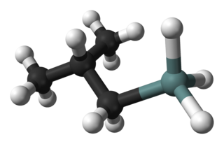
WIsobutylgermane (IBGe, Chemical formula: (CH3)2CHCH2GeH3, is an organogermanium compound. It is a colourless, volatile liquid that is used in MOVPE (Metalorganic Vapor Phase Epitaxy) as an alternative to germane. IBGe is used in the deposition of Ge films and Ge-containing thin semiconductor films such as SiGe in strained silicon application, and GeSbTe in NAND Flash applications.
 W
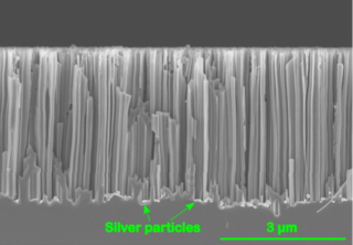
WMetal Assisted Chemical Etching is the process of wet chemical etching of semiconductors with the use of a metal catalyst, usually deposited on the surface of a semiconductor in the form of a thin film or nanoparticles. The semiconductor, covered with the metal is then immersed in an etching solution containing and oxidizing agent and hydrofluoric acid. The metal on the surface catalyzes the reduction of the oxidizing agent and therefore in turn also the dissolution of silicon. In the majority of the conducted research this phenomenon of increased dissolution rate is also spatially confined, such that it is increased in close proximity to a metal particle at the surface. Eventually this leads to the formation of straight pores that are etched into the semiconductor. This means that a pre-defined pattern of the metal on the surface can be directly transferred to a semiconductor substrate.
 W
WIn semiconductor electrochemistry, a Mott–Schottky plot describes the reciprocal of the square of capacitance versus the potential difference between bulk semiconductor and bulk electrolyte. In many theories, and in many experimental measurements, the plot is linear. The use of Mott–Schottky plots to determine system properties is termed Mott–Schottky analysis.
 W
WSemiconductor nanowire lasers are nano-scaled lasers that can be embedded on chips and constitute an advance for computing and information processing applications. Nanowire lasers are coherent light sources as any other laser device, with the advantage of operating at the nanoscale. Built by molecular beam epitaxy, nanowire lasers offer the possibility for direct integration on silicon, and the construction of optical interconnects and data communication at the chip scale. Nanowire lasers are built from III–V semiconductor heterostructures. Their unique 1D configuration and high refractive index allow for low optical loss and recirculation in the active nanowire core region. This enables subwavelength laser sizes of only a few hundred nanometers. Nanowires are Fabry–Perot resonator cavities defined by the end facets of the wire, therefore they do not require polishing or cleaving for high-reflectivity facets as in conventional lasers.
 W
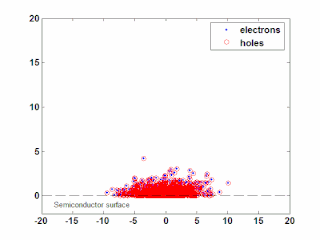
WIn semiconductor physics, the photo–Dember effect is the formation of a charge dipole in the vicinity of a semiconductor surface after ultra-fast photo-generation of charge carriers. The dipole forms owing to the difference of mobilities for holes and electrons which combined with the break of symmetry provided by the surface lead to an effective charge separation in the direction perpendicular to the surface. In an isolated sample, where the macroscopic flow of an electric current is prohibited, the fast carriers are slowed and the slow carriers are accelerated by an electric field, called the Dember field.
 W
WThe Rashba–Edelstein effect (REE) is a spintronics-related effect, consisting in the conversion of a bidimensional charge current into a spin accumulation. This effect is an intrinsic charge-to-spin conversion mechanism and it was predicted in 1990 by the scientist V.M. Edelstein. It has been demonstrated in 2013 and confirmed by several experimental evidences in the following years.
 W
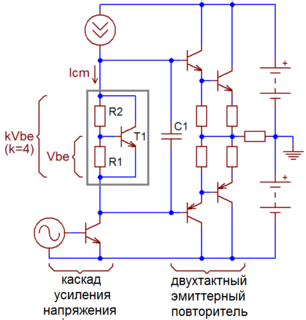
WIn electronics, a rubber diode or VBE multiplier is a bipolar junction transistor circuit that serves as a voltage reference. It consists of one transistor and two resistors, and the reference voltage across the circuit is determined by the selected resistor values and the base-to-emitter voltage (VBE) of the transistor. The circuit behaves as a voltage divider, but with the voltage across the base-emitter resistor determined by the forward base-emitter junction voltage.
 W
WSheet resistance, is a measure of resistance of thin films that are nominally uniform in thickness. It is commonly used to characterize materials made by semiconductor doping, metal deposition, resistive paste printing, and glass coating. Examples of these processes are: doped semiconductor regions, and the resistors that are screen printed onto the substrates of thick-film hybrid microcircuits.
 W
WSilver sulfide is an inorganic compound with the formula Ag2S. A dense black solid, it is the only sulfide of silver. It is useful as a photosensitizer in photography. It constitutes the tarnish that forms over time on silverware and other silver objects. Silver sulfide is insoluble in most solvents, but is degraded by strong acids. Silver sulfide is a network solid made up of silver and sulfur where the bonds have low ionic character.
 W
WSolid-state electronics means semiconductor electronics: electronic equipment using semiconductor devices such as transistors, diodes and integrated circuits (ICs). The term is also used for devices in which semiconductor electronics which have no moving parts replace devices with moving parts, such as the solid-state relay in which transistor switches are used in place of a moving-arm electromechanical relay, or the solid-state drive (SSD) a type of semiconductor memory used in computers to replace hard disk drives, which store data on a rotating disk.
 W
WSpin gapless semiconductors are a novel class of materials with unique electrical band structure for different spin channels in such a way that there is no band gap for one spin channel while there is a finite gap in another spin channel.
 W
WThe thermal copper pillar bump, also known as the "thermal bump", is a thermoelectric device made from thin-film thermoelectric material embedded in flip chip interconnects for use in electronics and optoelectronic packaging, including: flip chip packaging of CPU and GPU integrated circuits (chips), laser diodes, and semiconductor optical amplifiers (SOA). Unlike conventional solder bumps that provide an electrical path and a mechanical connection to the package, thermal bumps act as solid-state heat pumps and add thermal management functionality locally on the surface of a chip or to another electrical component. The diameter of a thermal bump is 238 μm and 60 μm high.
 W
WA topological insulator is a material that behaves as an insulator in its interior but whose surface contains conducting states, meaning that electrons can only move along the surface of the material. Topological insulators have non-trivial symmetry-protected topological order; however, having a conducting surface is not unique to topological insulators, since ordinary band insulators can also support conductive surface states. What is special about topological insulators is that their surface states are symmetry-protected Dirac fermions by particle number conservation and time-reversal symmetry. In two-dimensional (2D) systems, this ordering is analogous to a conventional electron gas subject to a strong external magnetic field causing electronic excitation gap in the sample bulk and metallic conduction at the boundaries or surfaces.
WA topological insulator is a material that behaves as an insulator in its interior but whose surface contains conducting states, meaning that electrons can only move along the surface of the material. Topological insulators have non-trivial symmetry-protected topological order; however, having a conducting surface is not unique to topological insulators, since ordinary band insulators can also support conductive surface states. What is special about topological insulators is that their surface states are symmetry-protected Dirac fermions by particle number conservation and time-reversal symmetry. In two-dimensional (2D) systems, this ordering is analogous to a conventional electron gas subject to a strong external magnetic field causing electronic excitation gap in the sample bulk and metallic conduction at the boundaries or surfaces.
WThe field-effect transistor (FET) is a type of transistor that uses an electric field to control the flow of current in a semiconductor. FETs are devices with three terminals: source, gate, and drain. FETs control the flow of current by the application of a voltage to the gate, which in turn alters the conductivity between the drain and source.